
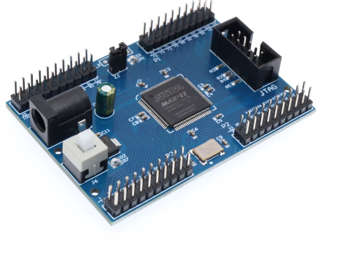
Altera MAX II EPM240 CPLD Development Board
$ 63.24


Description This development board is a classic “minimal system” for CPLD development. It is designed to be lean, providing the EPM240 chip and the bare essentials needed to get it running without the clutter of extra peripherals. 1. The Heart: EPM240T100C5 Chip The EPM240 belongs to the Altera (now Intel) MAX II family. Architecture: It is a CPLD based on a 0.18-µm flash process. Unlike an FPGA, the configuration is stored internally, making it non-volatile. Logic Density: It features 240 Logic Elements (LEs). While this sounds small compared to modern FPGAs, it is plenty for complex state machines, glue logic, or custom bus controllers. Package: The T100 suffix indicates a 100-pin Thin Quad Flat Pack (TQFP), which is relatively easy to probe if needed. 2. Communication & Clocking JTAG Interface: This is the standard 10-pin header used to connect a USB Blaster. It allows you to program the chip directly from Quartus and perform on-chip debugging. 50MHz Active Crystal: This provides a stable, high-speed heartbeat for your logic. In your HDL code (Verilog/VHDL), you will use this clock to drive counters, timers, or communication protocols. 3. Power Management AMS1117-3.3 Regulator: The EPM240 core and I/O typically operate at 3.3V. This regulator takes the 5V input (from the barrel jack or pins) and steps it down efficiently. Power Switch: A physical toggle to cut power without unplugging cables—a small but vital feature for hardware prototyping. 4. User Interaction & Expansion Programmable LED: Usually connected to a specific I/O pin (check your board’s schematic, often Pin 77 or similar). This is your “Hello World” tool to verify that your code is running. All I/O Exported: The board breaks out every usable pin to standard 2.54mm (0.1″) headers. This makes it breadboard-compatible and allows you to bridge the chip to external sensors, motors, or displays. Compact Size (5cm x 7cm): This small footprint makes it easy to embed into a larger project box or mount on a robot chassis.
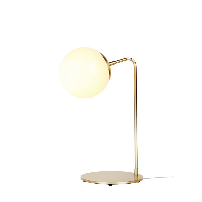
Related products
-
Sale!
 Select options
This product has multiple variants. The options may be chosen on the product page
Select options
This product has multiple variants. The options may be chosen on the product page
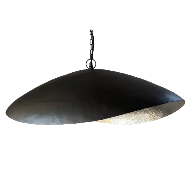
-
Sale!
 Select options
This product has multiple variants. The options may be chosen on the product page
Select options
This product has multiple variants. The options may be chosen on the product page
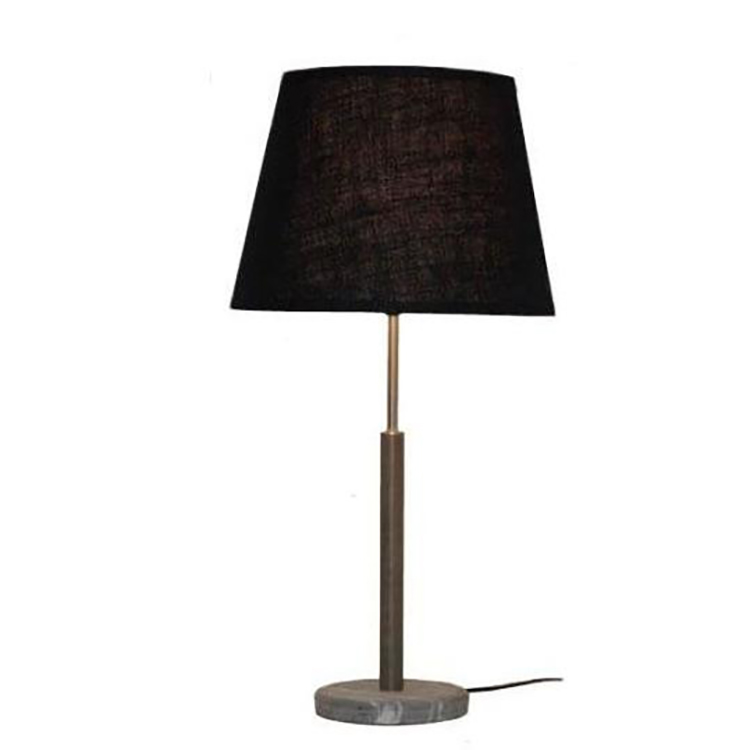
-
Sale!
 Select options
This product has multiple variants. The options may be chosen on the product page
Select options
This product has multiple variants. The options may be chosen on the product page
-
Sale!
 Select options
This product has multiple variants. The options may be chosen on the product page
Select options
This product has multiple variants. The options may be chosen on the product page